
AsianScientist (Jul. 31, 2015) – Scientists studying thin layers of phosphorus have found surprising properties that could open the door to ultrathin and ultralight solar cells and light emitting diodes (LEDs). Their research has been published in Light: Science and Applications.
The team used sticky tape to create single-atom thick layers, termed phosphorene, in the same simple way as the Nobel-prize winning discovery of graphene. But unlike graphene, phosphorene is a semiconductor, like silicon, which is the basis of current electronics technology.
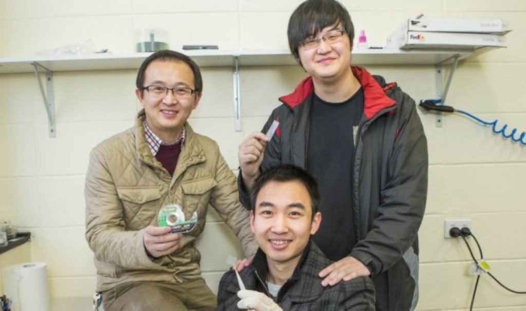
“Because phosphorene is so thin and light, it creates possibilities for making lots of interesting devices, such as LEDs or solar cells,” said lead researcher Dr. Lu Yuerui (Larry), from The Australian National University (ANU). “It shows very promising light emission properties.”
The team created phosphorene by repeatedly using sticky tape to peel thinner and thinner layers of crystals from the black crystalline form of phosphorus.
As well as creating semiconductors that are much thinner and lighter than silicon, phosphorene has light emission properties that vary widely with the thickness of the layers, which enables much more flexibility for manufacturing.
“This property has never been reported before in any other material,” said Lu. “By changing the number of layers we can tightly control the band gap, which determines the material’s properties, such as the color of LED it would make.”
“You can see quite clearly under the microscope the different colors of the sample, which tells you how many layers are there,” he added.
Lu’s team found the optical gap for monolayer phosphorene was 1.75 electron volts, corresponding to red light of a wavelength of 700 nanometers. As more layers were added, the optical gap decreased. For instance, for five layers, the optical gap value was 0.8 electron volts, a infrared wavelength of 1550 nanometres. For very thick layers, the value was around 0.3 electron volts, a mid-infrared wavelength of around 3.5 microns.
The behavior of phosphorene in thin layers is superior to silicon, said Lu.
“Phosphorene’s surface states are minimized, unlike silicon, whose surface states are serious and prevent it being used in such a thin state.”
The article can be found at: Yang et al. (2015) Optical Tuning of Exciton and Trion Emissions in Monolayer Phosphorene.
———
Source: Australian National University.
Disclaimer: This article does not necessarily reflect the views of AsianScientist or its staff.