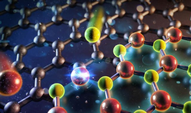
AsianScientist (May 22, 2019) – A research group in South Korea has developed a graphene-based high-performance transmission line with implications for high-speed semiconductor and communication devices. They published their work in the journal Advanced Functional Materials.
Due to the dense integration and high speed of semiconductor devices, the resistance of metal wires—in which signals among devices are transmitted—has increased geometrically, reaching the limit of permissible current density. To create the next generation of devices, carbon-based nanostructures such as graphene and carbon nanotubes have been proposed as substitutes for existing metal wires.
For instance, graphene, which consists of a hexagonal array of carbon only 0.3 nanometers thick, has electric conductivity that is 100 times greater than that of copper, and electron mobility that is 100 times faster than that of silicon. However, pure graphene has a low device concentration of 1012 per square centimeter, and its thinness results in very high electrical resistance.
Hence, researchers led by Professor Jang Jae Eun at the Daegu Gyeongbuk Institute of Science and Technology have combined graphene and amorphous carbon to increase the device concentration of graphene and enhance its electrical characteristics.
The team also proved that defects inside graphene decrease the frequency transmission of graphene, so they developed a stable doping technique that minimized internal defects of graphene during fabrication. The graphene-based transmission line displayed high signal transmission efficiency and stable operating characteristics, which could be useful to the semiconductor industry in the development of next-generation integrated circuits.
The article can be found at: Kang et al. (2019) Room Temperature Polariton Lasing in Quantum Heterostructure Nanocavities.
———
Source: RIKEN; Photo: Ben Mills/Wikimedia Commons/CC0.
Disclaimer: This article does not necessarily reflect the views of AsianScientist or its staff.


