
Dr. Arseniy Kuznetsov
Principal Scientist and Head of the Advanced Optical Technologies Department
Institute of Materials Research and Engineering (IMRE)
Agency for Science, Technology and Research (A*STAR)
Singapore
AsianScientist (Dec. 18, 2020) – From a projected Princess Leia pleading for help in the original Star Wars trilogy to Iron Man’s floating displays in the Avengers movies, holograms have long been a staple of science fiction. Though such sophisticated holograms remain out of reach, scientists like Dr. Arseniy Kuznetsov from the Agency for Science, Technology and Research (A*STAR) are working to make the technology an everyday reality, to benefit our economy and society.
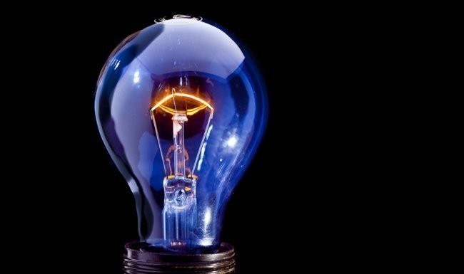
Holograms are created by recording light scattered by an object to reproduce a three-dimensional (3D) image. At A*STAR’s Institute of Materials Research and Engineering (IMRE), Kuznetsov studies how light behaves at the nanoscale—a field called nanophotonics. In 2012, his team showed that silicon nanoparticles act as miniscule antennas that can control light. Shining light on these so-called dielectric nanoantennas could then collectively supply the optical information needed to create high-resolution 3D holograms.
For his pioneering work in nanophotonics, Kuznetsov was recently elected a Fellow of the Optical Society of America. Speaking to Asian Scientist Magazine, Kuznetsov dives into his exciting research and shares his hopes for nanophotonics in the years to come.
- How would you summarize your research in a tweet?
Shaping light in an unusual way by using resonant nanoscale structures.
- Describe a completed research project that you are proudest of.
Between 2012-2013, my group in A*STAR pioneered a new branch of nanophotonics, related to dielectric nanoantennas. After demonstrating the fundamental properties of these systems, we started developing practical applications. Now, the field of dielectric nanoantennas is active worldwide with hundreds of papers published every year. More importantly, it demonstrates a huge potential for industrial application. Company engagements have already started and we expect to see the first products on the market in the next several years.
- What do you hope to accomplish with your research in the next decade?
We hope to bring the concepts of dielectric nanoantennas to the market in the next several years. Potential applications include: (1) new types of flat optical components for mobile devices, which can be more compact, lighter and cheaper than conventional optics, while providing enhanced functionalities; (2) Light Detection and Ranging (LiDAR) remote sensing systems for autonomous vehicles, robots and drones; (3) fully 3D holographic displays and many more.
- Who (or what) motivated you to go into your field of study?
Curiosity. Starting in light-matter interactions and later shifting to nanophotonics, I was always looking for areas that may impact science and technology significantly. I am thankful to my research mentors for helping me develop my passion for scientific novelty with practical impact. I am also very thankful to my family, for supporting me in my endeavors—even following me around the world. I could not have done it without their support.
- What is the biggest adversity that you experienced in your research?
Being disappointed, especially with past ideas that I placed my efforts into. Sometimes, your best scientific dreams can be crushed by new evidence. This is an unavoidable part of research, but it helps us move forward and shape our knowledge and skills. Accepting and understanding failures and learning from them is the best way towards real impact.
While I was in Germany, I worked on a method for fabricating and placing spherical nanoparticles made of different materials on a substrate, believing it could transform nanophotonics. But after I came to Singapore and did further research, I realized that the method was more or less useless, and conventional methods could do a much better job. This was disappointing. However, it was during this journey that I discovered the unusual optical properties of silicon nanoparticles, which then triggered my interest in my current field of dielectric nanoantennas. Even though my method failed to create an immediate impact, it enabled me to discover the properties of silicon nanoparticles and transition to the next stage of my career.
- What are the biggest challenges facing the academic research community today, and how can we fix them?
In the field of nanophotonics, the key challenge is showing that it can lead to real technologies and industrial impact. This is the direction we are currently working towards.
- If you had not become a scientist, what would you have become instead?
My answer would depend on the initial conditions. If I, with all my current knowledge and experience, was asked 20 years ago to choose something different with unlimited possibilities, I would probably choose industrial R&D or a company startup somewhere in Silicon Valley. However, if I consider my actual situation in Russia 20 years ago, I felt scientific work was the best way for me to achieve something in my life. Both my parents worked in a scientific institute, so this choice was quite obvious.
- What do you do outside of work to relax? Do you have any interests and hobbies?
Most of my free time I spend at home with my family—it does not mean we always play or communicate. Sometimes being together just means watching two different movies on two different iPads! I like to walk in Singapore’s nature resorts, and relax by listening to birds and cicadas. I also like to play the guitar and piano. For holidays, we travel for beach vacations or to visit our families in summer and ski in winter. For me, it is important to pursue different activities and maintain a healthy work-life balance to keep the energy high.
- If you had the power and resources to eradicate any world problem using your research, which one would you solve?
I would develop cost-effective and compact LiDAR solutions for autonomous driving and robotics. We can potentially make LiDARs so small and cheap that they can be integrated inside mobile devices. I believe our technology can also help to bring to reality 3D holographic displays, which can project fully 3D images without any additional glasses, like in the Iron Man films. These technologies could change the way we travel and how we interact with information.
- What advice would you give to aspiring researchers in Asia?
Be curious and self-driven. These will help you remove obstacles in the way and work towards your dreams. It is also important to find a topic you enjoy and will be passionate about. So dream big and don’t be afraid of failure. Every time you fall, learn from your experience, stand up and run forward to your goals!


This article is from a monthly series called Asia’s Rising Scientists. Click here to read other articles in the series.
———
Copyright: Asian Scientist Magazine; Photo: Arseniy Kuznetsov.
Disclaimer: This article does not necessarily reflect the views of AsianScientist or its staff.