
AsianScientist (Feb. 25, 2019) – Researchers in Singapore, the US and Russia have developed a machine learning approach that can predict changes to the properties of materials under strain. They published their findings in the Proceedings of the National Academy of Sciences.
When a semiconductor material is bent or strained, the atoms in its structure are perturbed, thus changing its properties, such as how it conducts electricity or transmits light. This process is known as strain engineering.
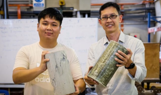
Conventional methods of studying and mapping the effects of strain engineering on a material rely on trial and error lab experiments and computer modeling on a limited scale. In the present study, scientists at Nanyang Technological University, Singapore, the Massachusetts Institute of Technology (MIT), US, and Skolkovo Institute of Science and Technology, Russia, combined the disciplines of material physics and artificial intelligence to better understand how material properties change under strain.
The researchers focused their efforts on semiconductors and explored the effect of reversible, nonlinear elastic strain on silicon-based materials. Identifying and applying the full potential of strain-engineered materials is very difficult due to the daunting range of possibilities, said the scientists. Strain can be applied in any of six different and independent ways, with nearly infinite gradations of degree, so the total number of possibilities are impractical to explore simply by trial and error.
“[The problem] quickly grows to 100 million calculations if we want to map out the entire elastic strain space,” said Professor Li Ju of MIT, who co-authored the study.
Using their neural network algorithm to automate these millions of calculations, the researchers were able to predict with high accuracy how different amounts and orientations of strain would affect the bandgap of semiconductor materials. Being able to tune the bandgap could improve the efficiency of semiconductor materials such as a silicon solar cell, increasing the energy harnessed from light while making it a thousand times thinner, thus reducing the cost of materials, transportation and infrastructure.
In addition to the bandgap, the machine learning method can also be used to study and predict other properties of materials, such as electronic, photonic and magnetic behaviors. The work points to potential new opportunities to create materials for electronic, optoelectronic and photonic devices that could be used for communications, information processing and energy applications.
The article can be found at: Shi et al. (2019) Deep Elastic Strain Engineering of Bandgap Through Machine Learning.
———
Source: Nanyang Technological University; Photo: Shutterstock.
Disclaimer: This article does not necessarily reflect the views of AsianScientist or its staff.