
AsianScientist (Oct. 31, 2017) – Scientists in Singapore have developed a device that can convert electrical signals into plasmonic signals with 1,000 times greater efficiency than existing methods. They published their findings in Nature Photonics.
Advancements in nanoelectronics have been fueled by the ever-increasing need to shrink the size of electronic devices to produce smaller, faster and smarter gadgets such as computers, memory storage devices, displays and medical diagnostic tools.
While most advanced electronic devices are powered by photonics—which involves the use of photons, or light particles, to transmit information—photonic elements are usually large in size, limiting their use in many advanced nanoelectronics systems.
Plasmons, which are waves of electrons that move along the surface of a metal after it is struck by photons, hold great promise for disruptive technologies in nanoelectronics. They are comparable to photons in terms of speed (they also travel at the speed of light) and are much smaller. This unique property of plasmons makes them ideal for integration with nanoelectronics. However, earlier attempts to harness plasmons as information carriers had little success.
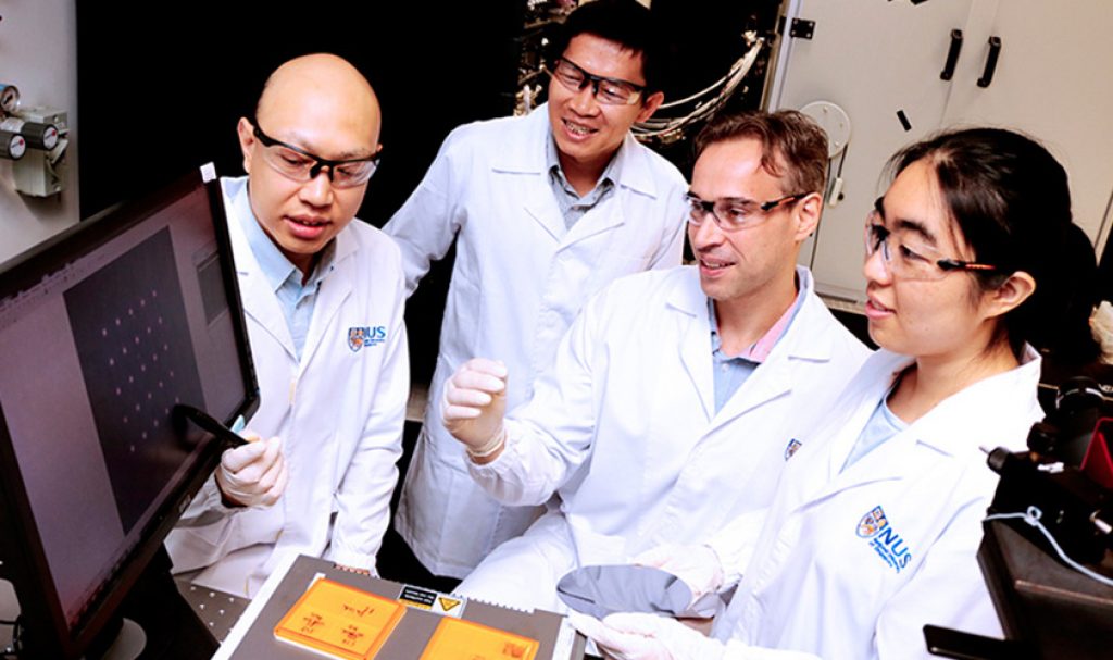
Addressing this technological gap, a research team from the National University of Singapore (NUS) has invented a converter that can harness the speed and small size of plasmons for high frequency data processing and transmission in nanoelectronics.
In conventional plasmonics, plasmons are excited in two steps—electrons are used to generate light, which in turn is used to excite plasmons. To convert electrical signals into plasmonic signals, and vice versa, in one single step, the team used a process called tunneling. This involves electrons travelling from one electrode to another, exciting plasmons in the process.
“The two-step process is time-consuming and inefficient. Our technology stands out as we provide a one-stop solution for the conversion of electrical signals to plasmonic signals,” explained study leader Associate Professor Christian Nijhuis.
“This can be achieved without a light source, which requires multiple steps and large optical elements, complicating integration with nanoelectronics. Based on our lab experiments, the electron-to-plasmon conversion has an efficiency of more than ten percent, more than 1,000 times higher than previously reported,” he added.
The research team has filed four patents for their invention and is collaborating with industry partners to integrate the plasmonic-electronic converters with existing technologies.
The researchers also plan to conduct further studies to reduce the size of the device so that it can operate at much higher frequencies. The team is even working on integrating the transducers with more efficient plasmonic waveguides for better performance.
“This innovative transducer can directly convert electrical signals into plasmonic signals, and vice versa, in a single step. By bridging plasmonics and nanoscale electronics, we can potentially make chips run faster and reduce power losses,” said Nijhuis.
“Our plasmonic-electronic transducer is about 10,000 times smaller than optical elements. We believe it can be readily integrated into existing technologies and can potentially be used in a wide range of applications in the future,” he added.
The article can be found at: Du et al. (2017) Highly Efficient On-chip Direct Electronic–plasmonic Transducers.
———
Source: National University of Singapore.
Disclaimer: This article does not necessarily reflect the views of AsianScientist or its staff.