
AsianScientist (Sep. 28, 2017) – A research team at the Korea Advanced Institute of Science and Technology (KAIST) has developed semiconductor manufacturing technology that makes use of a camera flash to produce patterns less than ten nanometers in size. The findings are published in the journal Advanced Materials.
Technology used in artificial intelligence, the internet of things and big data require high-capacity, high-performance semiconductor devices. It is therefore necessary to develop lithography technologies to produce such next-generation, highly integrated semiconductor devices. Although related industries have been using conventional photolithography for small patterns, this technique has limitations for forming patterns that are less than ten nanometers in size.
Molecular assembly patterning technology using polymers has been proposed as a replacement for photolithography because it is inexpensive and can easily form sub-ten nanometer patterns. However, heat treatment or toxic solvent vapor treatment used in molecular assembly patterning generally takes a long time. This makes mass production difficult and limits the commercialization of such technology.
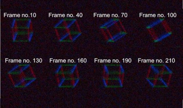
In this study, the research team introduced a camera flash in their protocol to produce a semiconductor pattern that was seven nanometers in size within 15 seconds. A single flash of light was sufficient to form molecular assembly patterns. The team also showed the compatibility of their technique with polymer flexible substrates, which opens the door to the fabrication of next-generation, flexible semiconductors.
“Despite its potential, molecular assembly semiconductor technology has remained a big challenge in improving process efficiency,” said Professor Kim Sang Ouk of KAIST who led the research. “This technology will be a breakthrough for the practical use of molecular assembly-based semiconductors.”
The article can be found at: Jin et al. (2017) Flash Light Millisecond Self-Assembly of High χ Block Copolymers for Wafer-Scale Sub-10 nm Nanopatterning.
———
Source: Korea Advanced Institute of Science and Technology.
Disclaimer: This article does not necessarily reflect the views of AsianScientist or its staff.