AsianScientist (Sep. 7, 2016) – A Japanese research team has developed a printing technique to form electronic circuits and thin-film transistors (TFTs) that have a line width and line spacing of 1 μm, or one millionth of a meter. Their work was published in the journal Advanced Materials.
Printed electronics—electronic devices fabricated using functional materials dissolved in ink—are drawing much attention in recent years as a promising new method to create large-area semiconductor devices and wearable devices at low cost. Thus, new printing techniques capable of consistently fabricating circuits with line widths of several micrometers or less are in great demand.
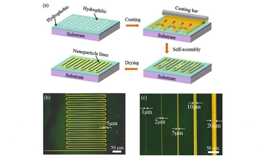
In this study, first author Dr. Liu Xuying and colleagues from the National Institute for Materials Science developed a printing technique capable of forming 1 μm wide metal circuits on flexible substrates. They used DryCure-Au, a metal nanoparticle ink that can form a conductive film at room temperature, to develop fully-printed organic TFTs with a channel length of 1 μm on flexible substrates.
In future studies, they aim to use the technique in applications such as large-area flexible displays and sensors. Other applications may also be possible in medical and bioelectronics fields, they say.
The article can be found at: Liu et al. (2016) Spontaneous Patterning of High-Resolution Electronics via Parallel Vacuum Ultraviolet.
———
Source: National Institute for Materials Science.
Disclaimer: This article does not necessarily reflect the views of AsianScientist or its staff.