AsianScientist (Nov. 4, 2014) – Researchers from the Graduate School of Nanoscience and Technology (GSNT) at the Korea Advanced Institute of Science and Technology (KAIST) have developed a method to obtain helical nanostructures through a self-assembly processes. Their results were published in the Proceedings of the National Academy of Sciences.
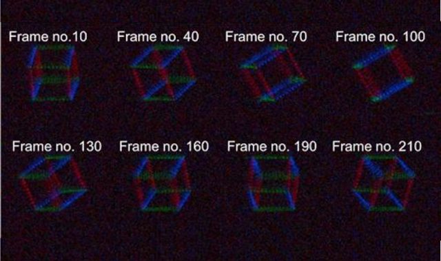
Considered one of the most difficult three-dimensional structures to form on the nano-scale, the helices were formed simply by using a confined area of 20 to 300 nanometers. The researchers were also able to vary the turns of the helices by varying the diameter of the confined space.
The helical nanostructures were made from liquid crystal and are therefore sensitive to surrounding electromagnetic fields. As such, the researchers expect that their helical nanostructures will find applications in the manufacture of highly efficient optoelectronic devices.
Furthermore, this technology facilitates the development of three dimensional patterning technology beyond current semiconductor manufacturing methods which use two dimensional photolithography processes. Three-dimensional semiconductor devices are expected to store hundred times more data than current devices. They will also lower costs by simplifying manufacturing processes.
The essence of this research, “self-assembly in confined space,” refers to controlling complex nanostructures which can be synthesized from materials such as macromolecules, liquid crystal molecules and biomolecules in relation to surrounding environments including the temperature, concentration and pH.

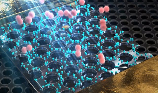
The research team produced a confined space with a length of tens of nanometers by using a porous anodized aluminum membrane induced from an electrochemical reaction. They successfully synthesized independently controlled helical nanostructures by forming the helical structures from liquid crystal molecules within that space.
“This research examines the physicochemical principle of controlling helical nanostructures. The technology enables the control of complex nanostructures from organic molecules by using confined space and surface reforming,” said Professor Yoon Dong-Ki, corresponding author of the present study.
“When grafted with nanotechnology or information technology, this technology will spur new growth to liquid crystal-related industries such as the LCD,” he added.
The article can be found at: Kim et al. (2014) Multistep Hierarchical Self-Assembly of Chiral Nanopore Arrays.
——-
Source: KAIST.
Disclaimer: This article does not necessarily reflect the views of AsianScientist or its staff.


