AsianScientist (Jul 30, 2014) – Using focused lasers, scientists have developed new techniques of modifying nanomaterials ranging from molybdenum disulfide (MoS2) sheets to silicon nanowires. The research papers documenting these findings have been published in ACS Nano and Scientific Reports, respectively.
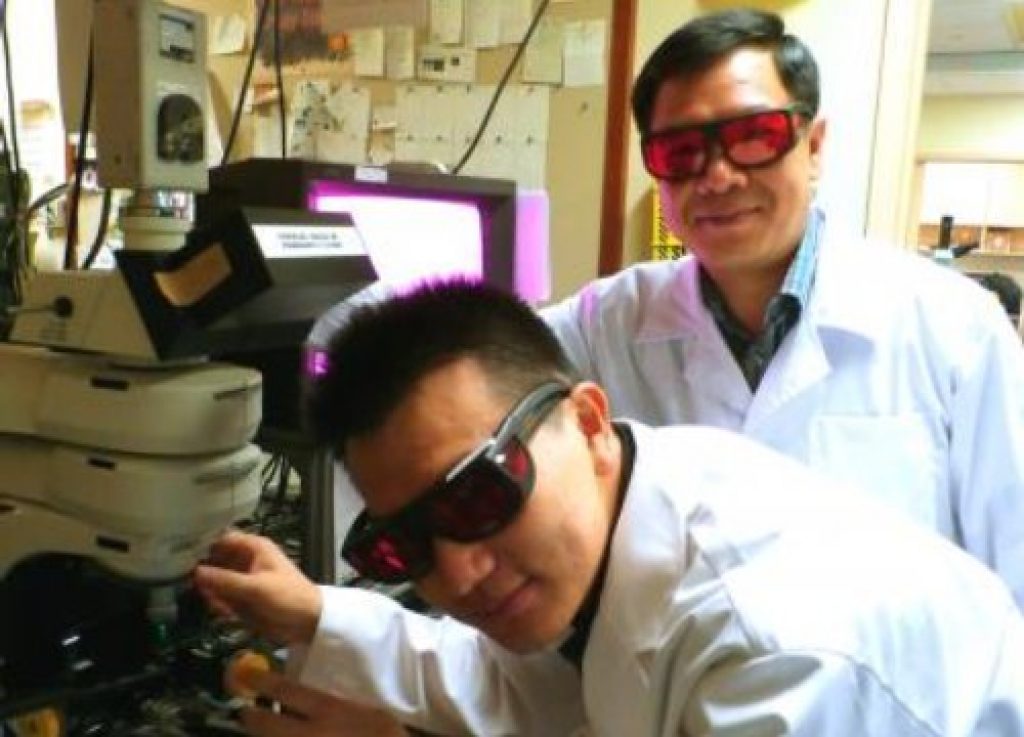
“In our childhood, most of us are likely to have the experience of bringing a magnifying glass outdoors on a sunny day and tried to focus sunlight onto a piece of paper to burn the paper. Such a simple approach turns out to be a very versatile tool in research. Instead of focusing sunlight, we can focus laser beam onto a wide variety of nanomaterials and study effects of the focused laser beam has on these materials,” said Professor Sow Chorng Haur from the Department of Physics at the National University of Singapore (NUS) who led the studies.
MoS2 has attracted great attention as a two-dimensional (2D) material that could be used in optoelectronics. One of the many fascinating properties of 2D MoS2 film is that its properties depend on the thickness of the film. In addition, its properties can be controlled through chemical modification. Therefore, one of the key challenges in the field of developing MoS2-based devices is fabricating components with different thicknesses or chemical structures.
To address this technological challenge, Prof. Sow and his team utilised an optical microscope-focused laser beam setup to ‘draw’ micropatterns directly onto large area MoS2 films as well as to thin the films.
With this simple and low cost approach, the scientists were able to use the focused laser beam to selectively ‘draw’ patterns onto any region of the film to modify properties of the desired area, unlike other current methods where the entire film is modified.
Interestingly, they also found that the electrical conductivity and photoconductivity of the modified material had increased by more than ten times and about five times respectively. The research team fabricated a photodetector using laser modified MoS2 film and demonstrated the superior performance of MoS2 for such application.
In a related study, Prof. Sow led another team of researchers from the NUS Faculty of Science, in collaboration with scientists from Hong Kong Baptist University, to investigate how ‘drawing’ micropatterns on mesoporous silicon nanowires could change the properties of the nanowires and advance their applications.
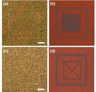
In one interesting application, the research team demonstrated that the micropatterns created at a low laser power are invisible under bright-field optical microscope, but become apparent under fluorescence microscope. This unique property could be used to create hidden images.
Prof. Sow and his team are looking to extend the versatile focused laser beam technique to more nanomaterials. In addition, they are investigating how to further improve the properties of MoS2 and mesoporous silicon with different techniques.
The articles can be found at:
Lu et al. (2014) Improved Photoelectrical Properties of MoS2 Films after Laser Micromachining.
Choi et al. (2014) Laser-induced Greenish-Blue Photoluminescence of Mesoporous Silicon Nanowires.
—–
Source: National University of Singapore.
Disclaimer: This article does not necessarily reflect the views of AsianScientist or its staff.