
AsianScientist (Feb. 15, 2018) – In a study published in NPG Asia Materials, researchers in Japan have devised a method to create two materials, each made of three layers of graphene.
In 2004, two scientists realized that they had isolated a single layer of carbon atoms on a sticky tape used to clean a graphite crystal. Since then, graphene has captured the imagination of researchers due to its fascinating properties—it is 200 times stronger than steel, is very flexible, and is an excellent conductor of electricity.
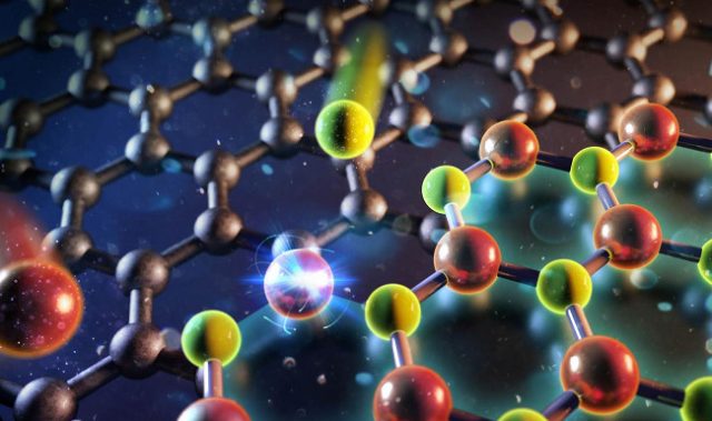
Graphene’s carbon atoms are arranged into hexagons, forming a honeycomb-like lattice. Placing one layer of graphene on top of another leads to the formation of bilayer graphene. The layers can be arranged in one of two positions: the centers of the carbon hexagons of each layer can be organized immediately above one another, called AA-stacking, or they can be displaced forwards so that a hexagon center in one layer is above a carbon atom below it, called AB-stacking. AB-stacking of two layers of graphene leads to the formation of a material with semiconducting properties when an external electric field is applied.
Deliberately stacking three layers of graphene has proven difficult, but doing so could help researchers study how the physical properties of tri-layered materials change based on how the layers are stacked. This could lead to the development of novel electrical devices.
In the present study, researchers at Japan’s Tohoku University and Nagoya University have fabricated two different types of trilayer graphene with different electrical properties. They heated silicon carbide using one of two methods. In one experiment, silicon carbide was heated to 1,510°C under pressurized argon. In another, it was heated to 1,300°C in a high vacuum.
Both materials were then sprayed with single hydrogen atoms. Two types of trilayer graphene then formed. The silicon carbide heated under pressurized argon formed into ABA-stacked graphene, in which the hexagons of the top and bottom layers were exactly aligned, while the middle layer was slightly displaced. The silicon carbide heated in a vacuum developed into ABC-stacked graphene, in which each layer was slightly displaced in front of the one below it.
The researchers then examined the physical properties of each material and found that their electrons behaved differently. The ABA graphene was an excellent electrical conductor, similar to monolayer grapheme. The ABC graphene, on the other hand, acts more like AB graphene in that it had semi-conductor properties.
“The present success in selective fabrication of ABA and ABC trilayer graphene would widen the feasibility of graphene-based nano-electronic devices with variable layer numbers and stacking sequences,” said the researchers.
The article can be found at: Sugawara et al. (2018) Selective Fabrication of Free-standing ABA and ABC Trilayer Graphene with/without Dirac-cone Energy Bands.
———
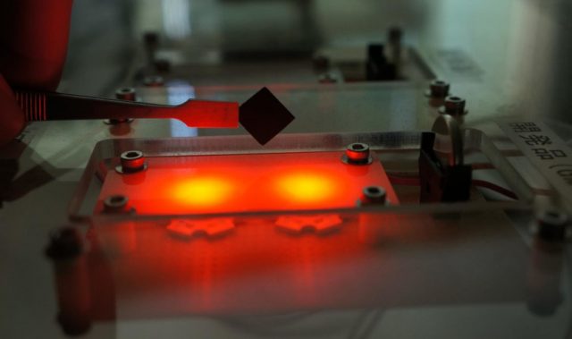
Source: Tohoku University; Photo: Shutterstock.
Disclaimer: This article does not necessarily reflect the views of AsianScientist or its staff.