AsianScientist (Sep. 28, 2017) – In a study published in Nature Nanotechnology, scientists have developed the first two-dimensional (2D) field-electronic transistors (FETs) by using a material that is both a metal and a semiconductor at once.
Modern life will be almost unthinkable without transistors. They are the ubiquitous building blocks of all electronic devices. For example, each computer chip contains billions of them. However, as the chips become smaller and smaller, the current 3D FETs are approaching their efficiency limit.
In simple terms, FETs can be thought of as high-speed switches, consisting of two metal electrodes and a semiconducting channel in between. Electrons move from the source electrode to the drain electrode, flowing through the channel. While 3D FETs have been scaled down to nanoscale dimensions successfully, the short semiconductor channel lengths lead to a decrease in performance—some electrons are able to flow between the electrodes even when they should not, causing heat and reducing efficiency.
To overcome this loss of performance, transistor channels have to be made using nanometer-scale thin materials. However, even thin 3D materials are not good enough, as unpaired electrons, part of the so-called ‘dangling bonds’ at the surface, interfere with the flowing electrons, leading to scattering.
In this study, a research team at the Center for Artificial Low Dimensional Electronic Systems within the Institute for Basic Science (IBS), has developed the first 2D FET made from a single material.
“FETs made from 2D semiconductors are free from short-channel effects because all electrons are confined in naturally atomically thin channels, free of dangling bonds at the surface,” explained Dr. Ho Sung Ji who was the first author of the study.
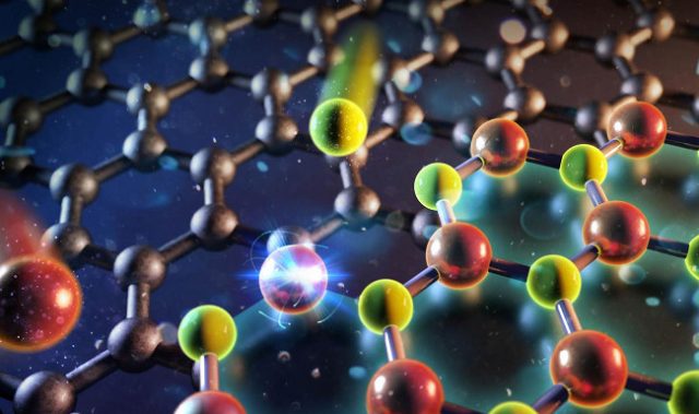
The researchers also sought to address a major issue of 2D FET transistors: the existence of a large contact resistance at the interface between the 2D semiconductor and any bulk metal. To reduce contact resistance, the team used molybdenum telluride (MoTe2) which functioned as both the semiconductor and the metal for the 2D transistor.
To build high quality metallic or semiconducting MoTe2 crystals, the researchers relied on a technique known as chemical vapor deposition. The shift between metal and semiconductor states was controlled by varying the temperature inside a hot-walled quartz-tube furnace filled with sodium chloride vapor. Raising the temperature to 710 degrees Celsius produced a metal, while a temperature of 670 degrees Celcius produced a semiconductor.
Contact resistance at the interface between the semiconductor and metallic MoTe2 was shown to be very low, and barrier height was lowered by a factor of seven, from 150 to 22 milli-electronvolts.
To showcase the versatility of their method, the scientists also manufactured larger scale structures using stripes of tungsten diselenide (WSe2) alternated with tungsten ditelluride (WTe2). They first created a thin layer of semiconducting WSe2 with chemical vapor deposition, then scraped out some stripes and grew metallic WTe2 in its place.
The researchers anticipate that in the future, it would be possible to reduce contact resistance even further, reaching the theoretical quantum limit.
The article can be found at: Sung et al. (2017) Coplanar Semiconductor–metal Circuitry Defined on Few-layer MoTe2 via Polymorphic Heteroepitaxy.
———
Source: Institute for Basic Science.
Disclaimer: This article does not necessarily reflect the views of AsianScientist or its staff.


