AsianScientist (Oct. 26, 2015) – With the exception of Sundays, long queues snake outside the Sistine Chapel every day of the week, with thousands of visitors to Vatican City waiting for their turn to catch a glimpse of Michelangelo’s masterpiece, The Last Judgement. A hush falls as the tourists turn their gaze heavenward, marveling at the ceiling fresco painted more than four centuries ago. Few, if any, pay notice to the light source enabling them to take in the finer details of Michelangelo’s work: light-emitting diodes or LEDs.
LEDs are quietly replacing traditional incandescent lighting the world over, not only places like the Sistine Chapel and museums such as the Louvre, but also in homes in both developed and developing countries. The reason is simple: LEDs are much more energy-efficient and last longer than incandescent light bulbs, and unlike fluorescent lights, do not use toxic mercury.
As far as the idea of using semiconductors to produce light goes, LEDs are not particularly novel, having first been developed in red and green in the 1950s. But it took 30 more years of research before scientists finally managed to produce blue LEDs, the Holy Grail which finally enabled the production of white light.
For this achievement, Shuji Nakamura, professor at the University of California, Santa Barbara (UCSB), was awarded the Millennium Technology Prize in 2006. Eight years later, Nakamura’s contributions were recognized once again, this time by the Nobel Foundation, which conferred on him the 2014 Nobel Prize in Physics along with co-discoverers Isamu Akasaki and Hiroshi Amano.
More light than heat
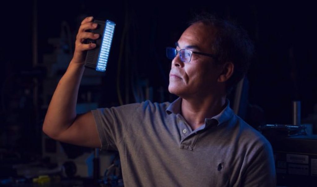
“The reason LEDs are so efficient is that they convert electricity directly into light,” Nakamura explained to Asian Scientist Magazine.
Incandescent light bulbs, in contrast, generate light indirectly by using electricity to heat up a tungsten filament until it starts to glow, reaching temperatures of about 2,000-3,300K (~1,700-3,000 °C).
In sensitive lighting applications, the excess heat generation is not only wasteful, but could also damage the artifacts. Furthermore, only about ten percent of the light that incandescent bulbs give off fall in the visible spectrum—the remaining infrared and ultraviolet radiation do not help illuminate objects and yet contribute to the degradation of photosensitive pigments.
LEDs are made using layers of semiconductor material, typically alloys of gallium and other metals. One layer, the negatively charged n-layer, is designed to have excess electrons, while the positively charged p-layer has ‘holes’ which accept electrons. When a current is passed through the LED, electrons and holes are driven to the active layer where they combine, emitting light in the process.
The exact wavelength of light emitted, and consequently the color perceived, is determined by bandgap between the semiconductor materials used in the n- and p-layers. Aluminum gallium arsenide, for example, produces red light, while gallium phosphide can be doped to produce light ranging from orange to green. A material to produce blue light, however, proved to be much more elusive.
Keeping it contrarian
The problem of producing blue LEDs captivated Nakamura, who had joined the R&D department of Nichia Chemical Industries Ltd. after receiving his master’s degree in 1979. Today one of the leading LED manufacturers in the world, Nichia was at that time focused on phosphors for cathode ray tubes and fluorescent lights.
Nakamura knew that finding the right material would take LEDs out of simple calculator displays and into the exciting new realm of solid state lighting. But first things first, he had to get his PhD. Along the way, he would make a decision that has shaped the development of LED lighting ever since.
“In 1988, I was sent to the University of Florida as a visiting researcher for a year. The senior lab members and PhD students I was working with there asked me whether I had published any papers. When I told them I hadn’t, they treated me like a technician,” Nakamura shared. He decided then and there that he would make getting a PhD his top priority.
“It was possible at that time to get a PhD degree without going to university; you just had to publish at least five research papers. Looking at the field, I saw that there were many papers being published on zinc selenide, making it impossible for me to make my mark there. On the other hand, there were only a few papers looking at gallium nitride (GaN). This is why I selected gallium nitride.”
The choice proved to be fortuitous. GaN was not a popular choice at the time: it was a fragile and finicky material that was considered impossible to grow to sufficient quality and quantity. Furthermore, it was extremely difficult to control the doping of GaN required to turn it into a p-layer, an essential step for making any diode.
But at Nagoya University, Nakamura’s Nobel coawardees Akasaki and Amano were patiently chipping away at the technical issues. By 1986, they had produced the first high-quality GaN crystal by using a thin layer of aluminum nitrite as a nucleus on a sapphire substrate. They also noticed that the GaN diode glowed more brightly when viewed under the scanning electron microscope, suggesting that electron beams could improve the intensity of GaN-based LEDs.
Nakamura, however, found his own way around the challenge, joining the fray in 1989. Instead of using aluminum nitrite as a seed, he grew the first layer of GaN at low temperature and subsequent layers at the high temperatures required for high-quality crystals. Furthermore, he devised a much cheaper workaround than the scanning electron microscope, creating a functional GaN p-layer with simple heating.
Growing high-quality GaN was not enough, unfortunately. The light produced by early blue LEDs was too dim to be of practical use. Due to differences in how the two different materials expand in response to temperature, GaN grown on a sapphire substrate had too many structural defects, with a dislocation density of more than 1010 per cm3. But if indium gallium nitride was used instead as the emitting layer between the GaN n- and p-layers, bright blue light was emitted.
“We still don’t fully know why indium gallium nitride gives such bright emission despite the huge number of dislocation defects in GaN,” Nakamura said. “Indium gallium nitride is a miracle material; I was lucky to have found it.”
Nakamura v. Nichia
Nakamura was not as lucky on the employment front. With the commercial release of the high-brightness blue LEDs in 1994, Nichia pivoted from phosphors to become one of the world’s leading LED manufacturers, ahead of larger, more established companies. Nakamura’s compensation for his role in the discovery? A ‘bonus’ of US$180.
Disheartened, Nakamura finally left Nichia after 20 years of service, moving to the United States to continue doing research at the University of California, Santa Barbara. Then in 2001, he did what was unthinkable for any Japanese salaryman, he filed a lawsuit against his ex-company, asking for a share of the royalties that amounted to US$180 million.
“It was actually a countersuit,” Nakamura clarified. “Nichia had sued me in late 2000 for infringement of trade secrets.”
What followed was a high-profile legal case, extensively covered by Japanese and international media. Estimating that Nichia had earned profits to the tune of ¥120 billion (~US$1 billion) from Nakamura’s invention, a Tokyo District Court ruled that they should pay him at least half that amount. Nichia appealed, and after long-drawn legal proceedings, managed to settle at ¥844 million (~US$8 million) in 2005.
The case was not just vindication for Nakamura but had a profound impact on the way inventors are treated in Japan today. It sparked a discussion on the unquestioned balance of power between employer and employee, and its impact on innovation.
“Before my lawsuit against Nichia, all Japanese companies usually gave the inventor a special bonus of US$10,000. After my lawsuit, all companies changed their policies and now the good ones give about US$3 million and about one percent of the royalties. These are some of the positive things that came out of the lawsuit,” Nakamura said.
Unfortunately, Nakamura’s case has also brought about some unintended consequences. Shaken by Nichia’s unprecedented payout, Japanese companies banded together under the Keidanran (Japanese Business Federation) to pressurize the government to change patent laws, specifically article 35, which assigns patents to individual inventors rather than their employers.
In July 2015, the Japanese House of Councilors passed a bill allowing companies to obtain patents on their employees’ inventions. Designed to reduce companies’ litigation risks, the amendment was the first in more than 90 years.
Switching substrates
Lawsuit notwithstanding, Nakamura continued to keep up his relentless work ethic in his new academic environment at UCSB. Working with colleagues Steven DenBaars and Jim Speck, Nakamura reported another breakthrough in 2007: the first non-polar blue-violet laser diodes.
Blue-violet lasers, with much shorter wavelengths than the red lasers used in regular DVD players, enable Blu-ray discs to pack in five times as much information as normal DVDs. Nakamura’s non-polar lasers were superior, with ten times the current density than the commercially-available blue lasers used in Blu-ray players.
Unlike LEDs, where the light is emitted in all directions, laser light is highly focused, with all photons moving ‘in step’ with each other. Although GaN has a suitable bandgap for producing blue laser light, the c-plane orientation of GaN crystals grown on sapphire meant that it suffered from strong polarization fields, greatly reducing the laser’s output.
To overcome these issues, Nakamura and his team replaced the sapphire substrate with GaN itself, pioneering what he calls GaN-on-GaN technology. By using GaN crystals in the m-plane orientation as the substrate, he was able to grow non-polar GaN crystals. These non-polar GaN crystals not onlcircumvented the polarization problem, but also had much fewer dislocations and other defects than GaN grown on sapphire, silicon carbide or any other commercially-used substrates.
Starting up Soraa
Beyond the field of semiconductor research, Nakamura’s work caught the attention of investors. One of them was Vinod Khosla, billionaire founder of clean tech-focused venture capitalist firm Khosla Ventures and co-founder of technology giant Sun Microsystems.
With Khosla’s backing, Nakamura, DenBaars and Speck stealth-launched Soraa in 2008. The company flew under the radar while assembling a management team and working on the underlying tech, only announcing their first product, the MR16 lamp, in 2012. By that time, the company had raised some US$100 million in venture capital funding.
“Beyond current densities of about 100 amperes per square centimeter, conventional GaN LEDs experience a phenomenon called droop, where the efficiency experiences a dramatic drop at higher power. This meant that to make a bright LED, many LED chips need to be used together in an array,” Nakamura explained.
“The c-plane GaN used in the MR16 has a dislocation density 1,000 times lower than GaN grown on sapphire, allowing it to operate at a much higher current density of 250 amperes per square centimeter.”
Soraa’s GaN-on-GaN lamps target the high-end market and are currently in use in retail outlets, residential projects and yes, museums too—the Victoria and Albert Museum in London, for example. But it remains to be seen whether the average consumer is discerning enough to notice the difference and be willing to pay for the quality that Soraa offers.
In a bid to lower prices, other leading LED producers like Cree Inc. and OSRAM Opto Semiconductors GmbH have placed their bets on silicon carbide and silicon as cheaper substrates more suitable for mass production. The stakes are high, with the global LED lighting market predicted to be worth US$25.7 billion in 2015.
But whether or not Nakamura’s bet on GaN turns out to be successful the second time around, his place in history is secure. Used in everything from the ubiquitous smartphone and LCD screens, to phototherapy for babies born with jaundice and water sterilization devices, his invention has already touched the lives of billions of people and changed the way we view the world.
This article was first published in the print version of Asian Scientist Magazine, October 2015
———
Photo: Matt Perko, University of California, Santa Barbara.
To read more, subscribe to Asian Scientist Magazine in print and receive four issues of Asian Scientist Magazine delivered directly to your mailing address for 12 months, inclusive of taxes and postage.


