AsianScientist (Jul. 22, 2011) – Japanese researchers report in the journal Nature a new technique for printing thin film transistors, called InkJet technology.
Researchers from the National Institute of Advanced Industrial Science and Technology (AIST) in Tsukuba, Japan hoped to get around the problem of self-crystallization, inherent in other InkJet/transistor making processes, which results in spreading effects that make it difficult to print uniformly.
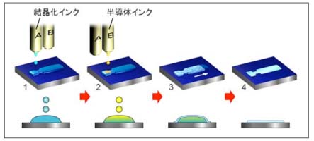
The team developed a two-step process, whereby one type of ink is sprayed first onto a substrate followed by another immediately afterwards, directly on top of the first. As the inks mix, they create an environment whereby one single crisp and sharp crystal grows and adheres to the material it is printed on.

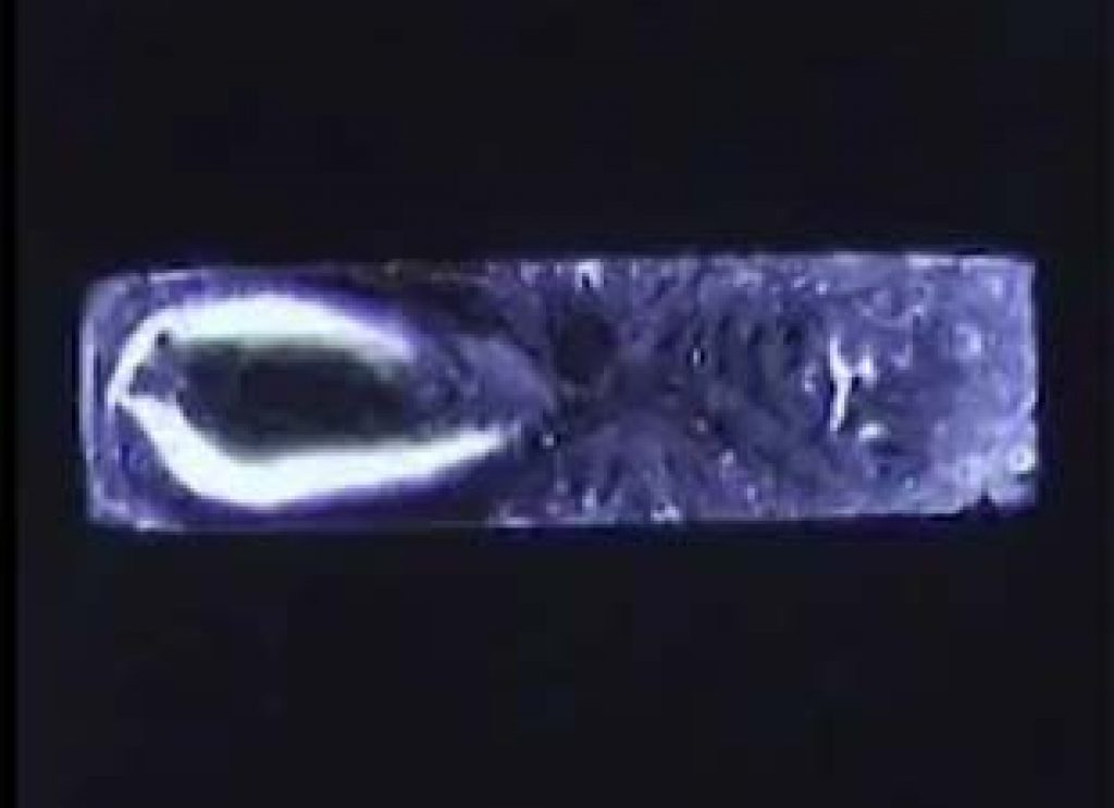
As soon as the crystal forms, it keeps on growing until the entire pool of ink is consumed, resulting in a thin film (30-200 nm thick) affixed to the substrate. After printing a complete pattern with their new process onto a substrate, other components were added to complete the transistor.
The researchers hope that their InkJet sprayed transistor technology may lead to a whole host of products that are based on bendable substrates, such as flexible displays, solar cells, large sheets of sensors, or true ePaper.
They plan to look into whether their new technique could also be used to create metal wires which would allow for a transistor to be made entirely from InkJet spraying technology.
The YouTube video of the InkJet sprayed transistor technology (in Japanese):
The article can be found at: Minemawari H et al. (2011) Inkjet printing of single-crystal films.
—–
Source: PysOrg.com.
Disclaimer: This article does not necessarily reflect the views of AsianScientist or its staff.


