
AsianScientist (Dec. 19, 2013) – Researchers from the National University of Singapore (NUS) have successfully developed a one-step method to grow and transfer high-quality graphene on silicon and other stiff substrates, opening up opportunities for graphene to be used in high-value applications that are currently not technologically feasible.
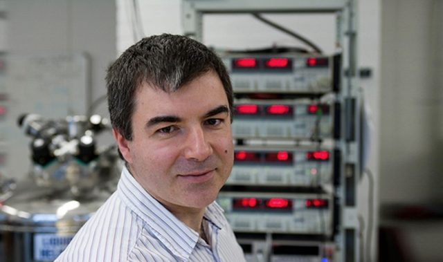
The study, led by Professor Loh Kian Ping who heads the Department of Chemistry at the NUS Faculty of Science, was published in the scientific journal Nature.
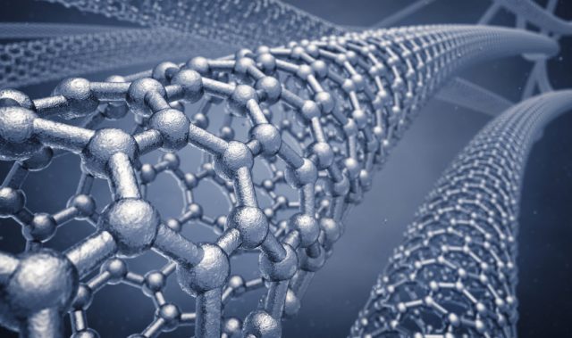
Graphene has attracted a lot of attention in recent years because of its outstanding electronic, optical and mechanical properties, as well as its use as transparent conductive films for touch screen panels of electrodes. However, the production of high quality wafer-scale graphene films is beset by many challenges, among which is the absence of a technique to grow and transfer graphene with minimal defects for use in semiconductor industries.
“Although there are many potential applications for flexible graphene, it must be remembered that to date, most semiconductors operate on “stiff” substrates such as silicon and quartz,” said Professor Loh.
“The direct growth of graphene film on silicon wafer is useful for enabling multiple optoelectronic applications, but current research efforts remain grounded at the proof-of-concept stage. A transfer method serving this market segment is definitely needed, and has been neglected in the hype for flexible devices.”
To address the current technological gap, the research team drew their cues from how beetles and tree frogs keep their feet attached to fully submerged leaves, and developed a new process called “face-to-face transfer.”
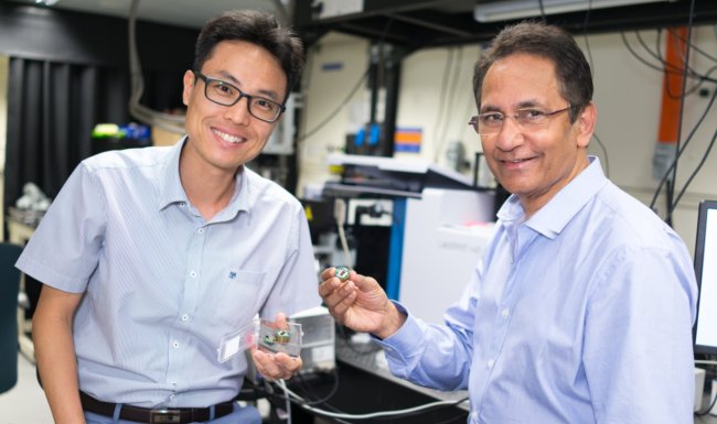
Dr. Gao Libo, the first author of the paper and a researcher with the Graphene Research Center at NUS Faculty of Science, grew graphene on a copper catalyst layer coating a silicon substrate.
After growth, the copper is etched away while the graphene is held in place by bubbles that form capillary bridges, similar to those seen around the feet of beetles and tree frogs attached to submerged leaves. The capillary bridges help to keep the graphene on the silicon surface and prevent its delamination during the etching of the copper catalyst. The graphene then attaches to the silicon layer.
To facilitate the formation of capillary bridges, a pre-treatment step involving the injection of gases into the wafer was applied by Dr. Gao. This helps to modify the properties of the interface and facilitates the formation of capillary bridges during the infiltration of a catalyst-removal liquid. The co-addition of surfactant helps to iron out any folds and creases that may be created during the transfer process.
The technique of growing graphene directly on silicon wafers and other stiff substrates may be useful for the development of rapidly emerging graphene-on-silicon platforms, which have shown a promising range of applications. The “face-to-face transfer” method developed by the NUS team is also amenable to batch-processed semiconductor production lines, such as the fabrication of large-scale integrated circuits on silicon wafers.
To further their research, Professor Loh and his team will optimize the process in order to achieve high throughput production of large diameter graphene on silicon, as well as target specific graphene-enabled applications on silicon. The team is also applying the techniques to other two-dimensional films. Talks are now underway with potential industry partners.
The article can be found at: Gao L et al. (2013) Face-to-face transfer of wafer-scale graphene films.
——
Source: National University of Singapore.
Disclaimer: This article does not necessarily reflect the views of AsianScientist or its staff.