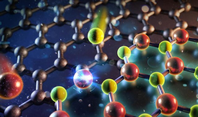

AsianScientist (Feb. 17, 2017) – By sandwiching a layer of graphene between the metal and semiconductor, researchers at the Ulsan National Institute of Science and Technology (UNIST) have greatly enhanced the performance of Schottky diodes. Their findings, published in Nano Letters, are expected to contribute to the semiconductor industry.
The Schottky diode is one of the oldest and most representative semiconductor devices, formed by the junction of a semiconductor with a metal. However, due to the atomic intermixing along the interface between two materials, it has been impossible to produce an ideal diode. An ideal diode acts like a perfect conductor when voltage is applied forward biased and like a perfect insulator when voltage is applied reverse biased.
Professor Park Kibog solved this problem by inserting a layer of graphene at the metal-semiconductor interface. In the study, the research team demonstrated that this graphene layer can not only suppress the material intermixing substantially, but also matches well with the theoretical prediction.
“The sheets of graphene in graphite have a space between each sheet that shows a high electron density of quantum mechanics in that no atoms can pass through,” said Park. “Therefore, with this single-layer graphene sandwiched between metal and semiconductor, it is possible to overcome the inevitable atomic diffusion problem.”
“In the case of silicon semiconductors, the electrical properties of the junction surfaces hardly change regardless of the type of metal they use,” explained Mr. Yoon Hoon Hahn, the first author of the study.
The article can be found at: Yoon et al. (2017) Strong Fermi-Level Pinning at Metal/n-Si(001) Interface Ensured by Forming an Intact Schottky Contact with a Graphene Insertion Layer.
———
Source: Ulsan National Institute of Science and Technology.
Disclaimer: This article does not necessarily reflect the views of AsianScientist or its staff.