
AsianScientist (May 16, 2011) – Scientists from Denmark, China, and the U.S. have reported in the journal Science a new method for revealing a 3D picture of the structure inside a material.
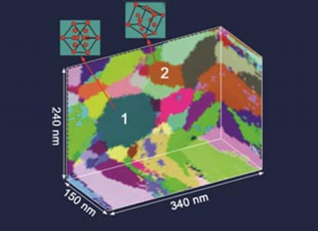
Most solid materials are composed of millions of small crystals packed together to form a fully dense solid. The orientations, shapes, sizes, and relative arrangement of these crystals are important in determining many material properties.
Traditionally, it has only been possible to see the crystal structure of a material by looking at a cut surface, giving just 2D information.
In recent years, x-ray methods have been developed that can be used to look inside a material and obtain a 3D map of the crystal structure. These methods have a resolution limit of around 100 nm (one nanometer is 100,000 times smaller than the width of a human hair).
This 100 nm resolution limit is not a problem for investigations of crystal structures inside nanomaterials, where the average crystal size is less than 100 nanometers.
An important advantage of such 3D methods is that they allow the changes taking place inside a material to be observed directly with a resolution 100 times better than existing non-destructive 3D techniques.
The article can be found at: Liu HH et al. (2011) Three-Dimensional Orientation Mapping in the Transmission Electron Microscope.
——
Source: Technical University of Denmark.
Disclaimer: This article does not necessarily reflect the views of AsianScientist or its staff.